
Europe’s Photonic Chips Strategy for Future AI
We are standing at a quiet, momentous precipice in hardware engineering. For decades, our digital existence has hummed to the rhythm of electrons dashing through silicon. Every smartphone notification, every binge-watched series, and every heavy-duty computation executed by hyper-scale server farms relies on this well-trodden electrical path. Yet, physics is stubborn. As transistors shrink to atomic scales, heat and resistance mount an aggressive defense against further progress.
Photonic chips process data using light instead of electricity, making them significantly faster, more energy-efficient, and capable of generating less heat than traditional electronic microchips. Europe is heavily investing in pilot manufacturing lines to position itself as a global leader in optical semiconductor production.<\/p>
- The Light Advantage: Photonic chips substitute electrons with light photons, dramatically reducing energy consumption and latency while boosting data speeds.
- The €400m PIX Europe Initiative: The European Union is driving domestic manufacturing capability to bypass heavy reliance on Asian and American semiconductor supply chains.
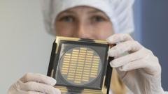
- Scaling to Six Inches: Dutch research institute TNO is leading an Eindhoven-based project to transition photonic wafer production from four inches to industrial six-inch scales by 2030.
Enter photonic chips. By swapping out electrical charges for beams of light, these revolutionary components offer a tantalizing glimpse into a hyper-fast, low-heat future. While still finding their footing outside specialized environments, they are steadily moving from university clean rooms into the commercial spotlight. And this time, Europe intends to lead the charge rather than play catch-up.
The Light-Speed Evolution of Optical Semiconductors
Talk to engineers working on optical hardware, and a familiar parallel immediately surfaces. The technology stands roughly where traditional electronic silicon stood forty or fifty years ago—pregnant with possibility, ripe for massive scaling, but still hampered by early-stage production bottlenecks. Industry experts at organizations like Reuters have noted how global powers are scrambling to secure the next major hardware paradigm.
Consider what makes optics so disruptive. Traditional microprocessors push billions of electrons through tiny circuits. That movement creates friction, and friction creates heat. Photons do not carry electrical charge in the same way. They travel without resistance penalties, meaning data moves faster, consumes a fraction of the power, and stays remarkably cool under immense computational strain.
“With optical chips, you are now where electronic chips were maybe 40 or 50 years ago. The demand is there, and the end goal is to have manufacturing in-house.” — Ton van Mol, TNO
The global race to commercialize this capability is fierce. While American firms like Coherent secure multi-million-dollar funding backed by heavyweights like Nvidia, Europe is mounting an aggressive, coordinated counter-offensive to capture the high-end hardware market.
Building a Continental Launchpad in Eindhoven
Europe’s ambitions are anchored firmly in the Netherlands, specifically on the High Tech Campus in Eindhoven. Backed by hundreds of millions of euros from the European Union and national coffers, a dedicated pilot line is taking shape. The goal? Scale production from the current global standard of four-inch wafers up to industrial six-inch indium phosphide wafers by 2030.
This is where structural geography matters. Just around the corner sits ASML, the Dutch titan holding a near-monopoly on the lithography machines required to build advanced semiconductors. Because photonic manufacturing shares immense procedural DNA with traditional semiconductor fabrication, ASML’s equipment and cleanroom processes will sit directly at the heart of the Eindhoven pilot line.
Comparing Semiconductor Manufacturing Paradigms
| Metric | Traditional Electronic Chips | Emerging Photonic Chips |
|---|---|---|
| Data Carrier | Electrons | Light Photons |
| Heat Generation | High (requires robust cooling) | Minimal |
| Standard Wafer Size | Up to 12 inches | Transitioning from 4 to 6 inches |
| Primary Current Use | General computing, mobile, AI | Data center interconnects, Lidar, sensors |
Former ASML chief executive Peter Wennink recently underscored the magnitude of this move, calling the pilot facility a vital launchpad for the continent’s digital economy. Rather than trying to rebuild every facet of legacy mass manufacturing—an impossible feat given high European labor costs and workforce constraints—the region is betting heavily on specialized ecosystems.
The Foundry Model: Democratizing Access
A major friction point for hardware startups has always been the immense capital expenditure required to build a fabrication plant. Building a modern chip foundry costs billions, pricing out innovative design firms before they ever leave the drawing board.
The Eindhoven project sidesteps this entirely by adopting a pure foundry model. The facility will not build proprietary branded products. Instead, it will manufacture photonic integrated circuits to order for external commercial clients.
- Open Access: Businesses across Europe and worldwide can utilize the pilot line.
- Cost Mitigation: Startups avoid sinking fortunes into private fabrication infrastructure.
- Standardized Yields: The objective is achieving a stable, highly reproducible manufacturing process by 2030.
By establishing this open foundry architecture, policymakers hope to replicate the foundational success that made Taiwan’s TSMC an indispensable linchpin of the global economy. If European entities control the primary fabrication pipelines for optical data transmission, future technological shifts—especially in hyper-scale artificial intelligence and next-generation 6G telecommunications—will naturally run through European infrastructure.
From Niche Sensors to Daily Realities
Today, photonic components are far from invisible, though they largely operate behind the scenes. They already power specialized enterprise infrastructure, handling optical data routing inside massive server complexes and guiding autonomous vehicles through sophisticated Lidar arrays. Yet, bringing them into consumer electronics—smartphones, laptops, and wearable diagnostic tech—requires solving severe manufacturing scale limitations.
That bottleneck is precisely what the current wave of investment aims to shatter. By transforming laboratory curiosities into high-yield, reproducible industrial products, engineers are laying the invisible tracks for the next half-century of computing. The electronic age built our modern world; the photonic wave is getting ready to propel it into light speed.
<button type="button" onclick="this.parentElement.innerHTML='✓ Thank you, we will refine our analysis!‘” style=”background:#ffffff; border:1px solid #cbd5e1; border-radius:6px; padding:4px 12px; font-size:12px; cursor:pointer; color:#334155;”>👎 No
